

A Comprehensive Introduction to Printed Circuit Boards (PCBs)
- Addtime: 2025-09-11 / View: 81
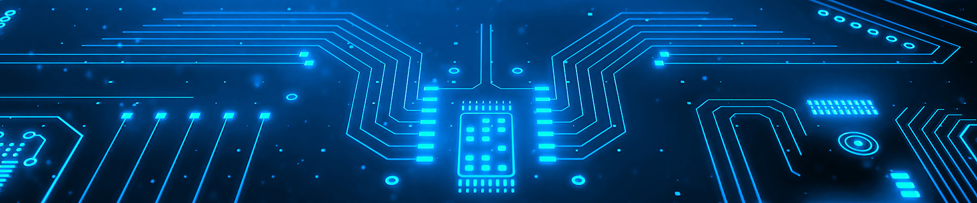
1.What is a PCB?
A Printed Circuit Board (PCB) is the foundational building block of most modern electronic devices. It is a non-conductive substrate sheet (typically made of fiberglass epoxy) with conductive pathways, tracks, or signal traces printed or etched from copper sheets. These pathways electrically connect and mechanically support electronic components.
Think of it as the nervous system and skeleton of an electronic device, providing structure and enabling communication between components.
2.The Main Parts of a PCB
Substrate (Laminate): The core material, usually FR-4 (a flame-retardant fiberglass epoxy). It provides the board with its rigid structure. Flexible PCBs use materials like Kapton.
Copper Layer: A thin layer of conductive copper foil laminated onto the substrate. Complex boards have multiple copper layers.
Solder Mask: The green (or other colors) polymer layer on top of the copper. It insulates the copper traces to prevent short circuits and protects the board from environmental damage.
Silkscreen: The white (or other colors) layer printed on top of the solder mask. It adds letters, numbers, symbols, and component outlines (component designators) for easier assembly and debugging (e.g., “R1” for the first resistor, “C5” for the fifth capacitor).
3.Types of PCBs
PCBs are classified by several factors:
By Number of Layers:
Single-Sided: Copper traces on only one side of the substrate. Simplest and cheapest.
Double-Sided: Copper traces on both sides. Components are mounted on both sides, and vias (plated-through holes) connect the two layers.
Multi-Layer (4, 6, 8… up to 50+ layers): Multiple layers of copper and substrate laminated together. Used in highly complex devices like smartphones and servers. Internal layers are dedicated to power and ground planes or complex signal routing.
By Flexibility:
Rigid: Standard rigid boards like FR-4.
Flexible (FPC): Made of flexible plastic. Used in wearables, cameras, and applications where space is limited or bending is required.
Rigid-Flex: A hybrid combining rigid and flexible sections. Common in high-end and military applications.
4.Key PCB Terminology
Pad: A small area of copper on a PCB where a component lead is soldered.
Via: A small plated hole that allows a connection between different copper layers.
Through-hole via: Goes through all layers.
Blind via: Connects an outer layer to an inner layer.
Buried via: Connects inner layers only (not visible from outside).
Trace: The copper “wire” that carries electrical signals between points.
Gerber Files: The standard file format (e.g., .gbr, .gbr.pho) used to communicate the PCB design to a manufacturer. They contain all the information for each layer (copper, solder mask, silkscreen).
Bill of Materials (BOM): A complete list of all components required to assemble the PCB, including reference designators, quantities, values, and part numbers.
Surface Mount Technology (SMT): A method where components are mounted directly onto the surface of the PCB. SMDs (Surface Mount Devices) are small and allow for very high component density.
Through-Hole Technology (THT): A method where component leads are inserted into drilled holes and soldered onto pads on the opposite side. Provides stronger mechanical bonds.
5.The PCB Manufacturing Process (Simplified)
Design: An engineer creates the schematic and board layout using ECAD (Electronic Computer-Aided Design) software (e.g., Altium Designer, KiCad, Eagle).
Printing/Plotting: The Gerber files are sent to the factory. A plotter uses them to create photomasks (films) for each layer.
Etching: A light-sensitive film is applied to the copper-clad substrate. The photomask is placed on top, and UV light hardens the desired pattern. Unhardened areas are washed away, and then a chemical etches away the exposed copper, leaving only the desired traces.
Lamination & Layer Alignment: For multi-layer boards, layers are stacked, aligned, and laminated together under high heat and pressure.
Drilling: Precise holes are drilled for vias and through-hole components.
Plating: The holes are plated with copper to create electrical connections between layers.
Solder Mask Application: The solder mask is applied, exposed to UV light through a mask, and developed to expose the pads.
Surface Finish: A finish (e.g., HASL, ENIG) is applied to the exposed copper pads to prevent oxidation and ensure good solderability.
Silkscreen Printing: The component labels and other markings are printed.
Electrical Test: A Flying Probe or Bed of Nails tester checks for short circuits and open connections to ensure the board was manufactured correctly.
Profiling & Routing: The individual PCBs are cut out from the larger production panel.
6. Design for Manufacturability (DFM)
A critical concept where the designer follows specific rules to ensure the board can be manufactured reliably and cost-effectively. This includes rules for trace width, spacing, hole size, and component placement. Ignoring DFM can lead to low yields, failures, and higher costs.